|
|

Loading ...
|
|
|
|
|
pages views since
05/19/2016 : 81169
· Members : 7
· News : 661
· Downloads : 0
· Links : 0
|
|
|
|
|
Using Blurred Light to 3D Print Superior Lenses
|
|
|
|
Posted by Okachinepa on 05/09/2024 @


Courtesy of SynEvol
Credit: Daniel Webber, National Research Council of Canada
Blurred tomography is a new 3D printing technique developed by researchers in Canada that can quickly create microlenses with optical quality suitable for commercial use. The new process could facilitate the design and fabrication of a wide range of optical devices more quickly and easily.
Daniel Webber of the National Research Council of Canada stated, "We purposely added optical blurring to the beams of light used for this 3D printing method to manufacture precision optical components." The creation of optically smooth surfaces is made possible by this.
The innovative technology is demonstrated by these researchers by creating a millimeter-sized plano-convex optical lens with imaging performance comparable to a commercially available glass lens, which they publish in Optica, the journal for high-impact research published by Optica Publishing Group. They also demonstrate how the process can yield optical components that are operational in 30 minutes or less.
"We believe that this approach will be beneficial for quick and inexpensive optical component prototyping because of the tomographic 3D printer's low cost and the materials it uses," stated Webber. Additionally, optical designers may be able to simplify designs by substituting printed optics with complicated shapes for many standard optics due to the intrinsic freeform nature of tomographic 3D printing.
Courtesy of SynEvol
Credit: Daniel Webber, National Research Council of Canada
A relatively recent manufacturing technique called tomographic volumetric additive manufacturing employs projected light to solidify a light-sensitive resin in particular locations. It enables the simultaneous printing of a whole part without the need for support structures. However, because the pencil-like beams used in these tomographic technologies generate striations that result in minor ridges on the component's surface, they are unable to print imaging-quality lenses directly. While smooth surfaces can be achieved with post-processing stages, this approach is more time-consuming and complex, negating the benefit of rapid prototyping that comes with tomographic printing.
According to Dr. Webber, "the complicated and time-consuming manufacturing process, coupled with the strict technical specifications required for a functioning lens, make optical component fabrication costly." "Freeform designs can be produced at a reasonable cost using blurred tomography. New optical devices might be prototyped considerably more quickly as technology advances, which would be helpful for both commercial producers and do-it-yourself inventors.
In order to evaluate the new technique, the scientists first constructed a basic plano-convex lens and demonstrated that its imaging resolution was on par with that of a commercial glass lens of the same physical dimensions. In addition, it displayed a point spread function near the glass lens, sub-nanometer surface roughness, and form error on the micron scale.
Additionally, they used blurring tomography to create a 3x3 array of microlenses, which they then compared to an array created using traditional tomographic 3D printing. They discovered that because of the high surface roughness of the array printed using traditional methods, it was not able to image a business card; nevertheless, this could be accomplished with the array printed using blurred tomography. The researchers also showed how to overprint a ball lens onto an optical fiber, which was previously only achievable with the use of two-photon polymerization, an additive manufacturing method.
Currently, they are trying to increase component accuracy by integrating material characteristics into the printing process and refining the light patterning technique. Moreover, they wish to automate the printing time so that the system is reliable enough for business use.
According to Webber, "tomographic 3D printing is a rapidly developing field that is finding use in many application areas." Here, we create millimeter-sized optical components by utilizing the inherent benefits of this 3D printing technique. By doing this, we have contributed a quick and inexpensive substitute to the toolkit of optical manufacturing processes that may influence future innovations.
|
|
|
|
A Quantum Computing Revolution Is Started by an Ultra-Pure Silicon Chip
|
|
|
|
Posted by Okachinepa on 05/07/2024 @
Courtesy of SynEvol
Credit: University of Melbourne/ University of Manchester
A revolutionary method for producing extremely pure silicon has been developed by researchers from the Universities of Manchester and Melbourne, taking the development of powerful quantum computers one significant step closer.
The researchers claim that the newly developed method for creating ultra-pure silicon makes it the ideal building block for producing quantum computers on a large scale and with excellent accuracy.
The innovation, which uses qubits of phosphorous atoms implanted into crystals of pure stable silicon, was reported in Communication Materials, a Nature journal. According to project co-supervisor Professor David Jamieson of the University of Melbourne, this could overcome a critical obstacle to quantum computing by extending the duration of infamously fragile quantum coherence.
Because of fragile quantum coherence, computation errors accumulate quickly. Professor Jamieson stated, "With the robust coherence our new technique provides, quantum computers could solve some problems that would take conventional or 'classical' computers - even supercomputers - centuries, in hours or minutes."
The fundamental units of quantum computing, known as qubits, are sensitive to minute alterations in their surroundings, such as variations in temperature. Current quantum computers can only sustain error-free coherence for a very short period of time, even when they are run in peaceful refrigerators close to absolute zero (minus 273 degrees Celsius).
Ultra-pure silicon, according to University of Manchester co-supervisor Professor Richard Curry, made it possible to build high-performance qubit devices, which are a crucial step toward the development of scalable quantum computers.
We have successfully created a crucial "brick" required for the construction of a quantum computer based on silicon. To create a technology that could revolutionize humankind, this is an essential first step, according to Professor Curry.
The key benefit of silicon chip quantum computing, according to lead author and joint Cookson Scholar of the Universities of Manchester and Melbourne, Ravi Acharya, is that it makes use of the same fundamental methods as modern computer chips.
"Billions of transistors make up an average computer's electronic chip; these transistors can also be used to build qubits for silicon-based quantum devices. The purity of the silicon starting material has been a limiting factor in the creation of high-quality silicon qubits thus far. We have the breakthrough purity here to fix this issue.
According to Professor Jamieson, the recently developed computer chips made of highly pure silicon house and safeguard qubits, allowing them to maintain quantum coherence for extended periods of time and reducing the need for error correction in complex operations.
"Our methodology paves the way for dependable quantum computing, which holds great potential for revolutionizing various aspects of society such as artificial intelligence, safe data and communication, medication and vaccine development, energy consumption, transportation, and production," the speaker stated.
The foundation material for today's information technology industry is silicon, which is derived from beach sand. It is a plentiful and adaptable semiconductor that, depending on what other chemicals are added to it, can function as an insulator or a conductor of electrical current.
Professor Jamieson stated, "While some are experimenting with other materials, we think silicon is the best option for quantum computer chips that will allow the long-lasting coherence needed for trustworthy quantum computations."
Courtesy of SynEvol
Credit: University of Melbourne/ University of Manchester
The issue is that while silicon found in nature largely consists of the desired isotope silicon-28, there is also roughly 4.5 percent silicon-29. According to him, silicon-29 has an additional neutron in the nucleus of each atom that functions as a tiny rogue magnet, shattering quantum coherence and causing computer mistakes.
In order to reduce silicon-29 from 4.5 percent to two parts per million (0.0002 percent), the researchers focused a high-speed, concentrated beam of pure silicon-28 on a silicon chip. This caused silicon-28 to gradually replace the silicon-29 atoms in the chip.
Professor Jamieson stated, "The good news is that we can now use an ion implanter, a common machine found in any semiconductor fabrication lab, tuned to a specific configuration that we designed, to purify silicon to this level."
In previously published work, the University of Melbourne set and maintains the world record for single-qubit coherence of 30 seconds using less pure silicon in collaboration with the ARC Centre of Excellence for Quantum Computation and Communication Technology. Complex quantum calculations can be completed in a reasonable amount of time—30 seconds.
According to Professor Jamieson, errors happened in milliseconds due to broken coherence, even though the largest quantum computers currently in use had over 1000 qubits.
The next challenge will be to show that we can maintain quantum coherence for numerous qubits at once after producing incredibly pure silicon-28. For certain applications, a dependable quantum computer with just 30 qubits may be more powerful than modern supercomputers, he claimed.
The Australian and UK governments provided research money to assist this most recent work. A Wolfson Visiting Fellowship from the Royal Society supports Professor Jamieson's work with the University of Manchester.
According to a 2020 CSIRO report, Australia may generate $2.5 billion in revenue annually and 10,000 employment using quantum computing by 2040.
|
|
|
|
Japanese Researchers Unveil Highly Effective Power Converter
|
|
|
|
Posted by Okachinepa on 05/07/2024 @
Courtesy of SynEvol
Credit:Mishima Tomokazu
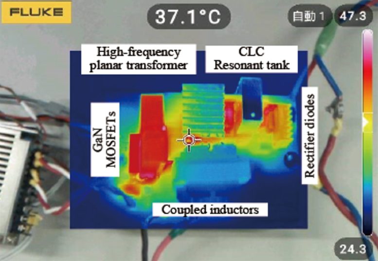
Kobe University has created a new electrical power converter design that offers much higher efficiency at lower cost and less maintenance. This direct current voltage boost converter is expected to have a significant influence on the advancement of electronic and electric components across a range of industries, including information technology, mobility, healthcare, and power generation.
One essential component unites all systems that use solar or vibration energy to power cars that run on hydrogen or power medical equipment. Low-voltage direct current input is transformed into high-voltage direct current output by this so-called "boost converter." It is ideal for it to use as few parts as possible for lower maintenance and expense, while also operating at maximum efficiency and producing no heat or electromagnetic noise, because it is such a fundamental and ubiquitous component. Boost converters' primary function is to swiftly switch between two circuit states—one for energy storage and the other for energy release.
The gadget as a whole can be made smaller by using smaller components due to faster switching. But doing so also produces more heat and electromagnetic noise, which lowers the power converter's efficiency.
Mishima Tomokazu, a power electronics researcher at Kobe University, and his team made great strides toward creating a novel direct current power conversion circuit. They were able to combine high-frequency switching—roughly ten times greater than previously—with "soft switching," a method of lowering electromagnetic noise and power losses from heat dissipation. They also managed to reduce the number of components, which kept costs and complexity down.
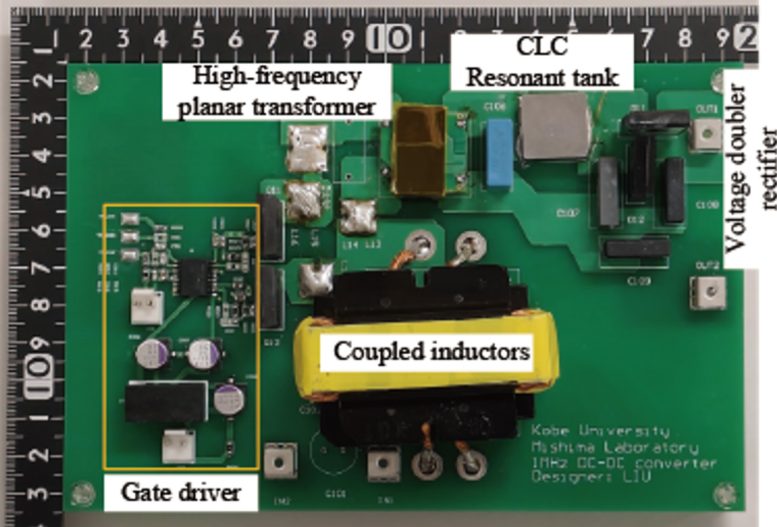
Courtesy of SynEvol
Credit:Mishima Tomokazu
There is a small moment when the switch is not fully closed when the circuit switches between two states, and during that moment, there is both a voltage and a current across the switch. This indicates that the switch dissipates heat during this period by functioning as a resistor. This dissipation increases with the frequency at which a switch state changes. According to Dr. Mishima, soft switching is a technique that minimizes heat loss by ensuring that switch transitions occur at zero voltage. This has traditionally been accomplished by "snubbers," which are parts that provide alternate energy sinks throughout the transition phase, causing energy losses in the process.
The innovative circuit design and assessment by the Kobe University team were published in the IEEE Transactions on Power Electronics journal. Their success can be attributed to their usage of "resonant tank" circuits, which have far lower losses since they can store energy during the switching phase. Furthermore, they employ a component-saving design known as a "planar transformer," which is incredibly tiny and has excellent thermal performance in addition to using flat components printed onto a circuit board.
Additionally, Mishima and his associates constructed a circuit prototype and assessed its functionality. We verified that, for an MHz drive with a high voltage conversion ratio, our snubberless design has significantly less electromagnetic noise and a high energy efficiency of up to 91.3 percent. Additionally, this ratio is more than 1.5 times larger than that of current designs. Nonetheless, scientists want to boost efficiency even more by lowering the magnetic components' power dissipation.
Given how commonplace electrical gadgets are in our daily lives, direct current power supply with a high voltage multiplier ratio must operate with great efficiency and low noise. Applications in electric power, renewable energy, transportation, information and telecommunications, and healthcare will benefit greatly from this Kobe University development. "The current development is a 100W-class small-capacity prototype, but we aim to expand the power capacity to a larger kW-class capacity in the future by improving the electronic circuit board and other components," Mishima says in explaining their future intentions.
|
|
|
|
How New Entanglement Control at MIT Is Redefining Quantum Computing
|
|
|
|
Posted by Okachinepa on 05/06/2024 @
Courtesy of SynEvol
Credit:Eli Krantz, Krantz NanoArt
One type of correlation that exists between quantum objects, like atomic-scale particles, is called entanglement. Though it is one of the characteristics that explains the macroscopic behavior of quantum systems, this peculiarly quantum phenomenon defies explanation by the rules of classical physics.
Gaining a greater understanding of entanglement could help scientists better grasp how information is stored and processed in quantum systems, as it is fundamental to their operation.
The fundamental components of a quantum computer are called qubits, or quantum bits. Nevertheless, creating distinct entangled states in many-qubit systems, let alone studying them, is quite challenging. Differentiating between the many entangled states might be difficult as well.
Researchers at MIT have now shown how to effectively create entanglement amongst a variety of superconducting qubits that behave in a particular way.
In recent years, scientists from the Engineering Quantum Systems (EQuS) group have worked on methods to accurately operate a quantum processor made out of superconducting circuits utilizing microwave technology. The methods presented in this work allow the processor to efficiently generate highly entangled states and transition those states between different types of entanglement, including those that are more likely to support quantum speed-up and those that do not. These control techniques are in addition to them.
"Here, we're showing that the developing quantum processors can be used as an instrument to deepen our knowledge of physics. The principal author of the study, Amir H. Karamlou '18, MEng '18, PhD '23, notes, "Although everything we did in this experiment was on a scale which can still be simulated on a classical computer, we have a good roadmap for scaling this technology and methodology beyond the reach of classical computing."
William D. Oliver, the director of the Center for Quantum Engineering, the head of the EQuS group, the Henry Ellis Warren professor of electrical engineering, computer science, and physics, and the associate director of the Research Laboratory of Electronics, is the senior author. Research Scientist Jeff Grover, postdoc Ilan Rosen, and other personnel from MIT's Electrical Engineering and Computer Science and Physics departments, as well as from MIT Lincoln Laboratory, Wellesley College, and the University of Maryland, join Karamlou and Oliver. The study was just released in the Nature journal.
Entanglement can be defined as the quantum information transferred between a subsystem of qubits and the remainder of the larger system in a large quantum system with many interconnected qubits.
A quantum system's entanglement can be classified as either area-law or volume-law according to the way this shared information scales with subsystem geometry. When there is volume-law entanglement, the degree of entanglement that exists between a qubit subsystem and the rest of the system increases in direct proportion to the subsystem's overall size.
However, area-law entanglement is contingent upon the number of common connections that a qubit subsystem has with the rest of the system. The degree of entanglement only increases along the subsystem's boundary with the larger system as it gets bigger.
Theoretically, the strength of quantum computing is associated with the creation of volume-law entanglement.
Oliver states, "We know that generating volume-law entanglement is a key ingredient to realizing a quantum advantage, even though we have not yet fully abstracted the role that entanglement plays in quantum algorithms."
Nevertheless, volume-law entanglement is also more difficult to simulate with a classical computer and practically prohibitive at scale compared to area-law entanglement.
Superconducting circuits, which are utilized to create artificial atoms, are a component of their processor. The artificial atoms are used as qubits, which are highly accurate devices that can be controlled and read out with microwave waves.
This experiment's apparatus had sixteen qubits placed in a two-dimensional grid. To ensure that each of the 16 qubits had the same transition frequency, the researchers meticulously adjusted the CPU. Subsequently, they concurrently applied a second microwave drive to each qubit.
This microwave drive creates quantum states with volume-law entanglement if its frequency matches that of the qubits. Nevertheless, the qubits show less volume-law entanglement with rising or decreasing microwave frequency, and eventually transition to entangled states that progressively follow an area-law scaling.
"Our study is a masterwork of superconducting quantum computing capabilities. In one experiment, Rosen adds, "we used the processor as a digital computing device to measure the entanglement scaling that resulted from operating it as an analog simulation device, which allowed us to prepare states with different entanglement structures efficiently."
The team worked diligently for years to carefully build up the infrastructure around the quantum processor in order to provide that control.
The crossover between volume-law and area-law entanglement was demonstrated, allowing the researchers to experimentally validate the predictions of previous theoretical studies. More crucially, this technique can be applied to identify as area-law or volume-law entanglement in a general quantum processor.
The difference between area-law and volume-law entanglement in two-dimensional quantum simulations with superconducting qubits is highlighted by the MIT experiment. Professor of theoretical physics at the University of Innsbruck Peter Zoller adds, "This beautifully complements our work on entanglement Hamiltonian tomography with trapped ions in a parallel publication published in Nature in 2023." Zoller was not involved in this work.
Pedram Roushan of Google, who was not involved in the study, states that "quantifying entanglement in large quantum systems is a challenging task for classical computers but a good example of where quantum simulation could help." Karamlou and colleagues measured the entanglement entropy of different subsystems of different sizes using a 2D array of superconducting qubits. By measuring the area-law and volume-law contributions to entropy, they may identify crossover behavior that occurs when the quantum state energy of the system is adjusted. It effectively illustrates the special insights that quantum simulators can provide.
This method could be used in the future by scientists to investigate the thermodynamic behavior of complicated quantum systems, which are currently too complex to examine analytically and are prohibitively expensive to model on even the most powerful supercomputers in the world.
"We may learn more about the nature of entanglement in these many-body systems, and the experiments we conducted in this work can be used to characterize or benchmark larger-scale quantum systems," says Karamlou.
|
|
|
|
2D Semiconductor Engineering is Transformed by Isotopes
|
|
|
|
Posted by Okachinepa on 05/06/2024 @
Courtesy of SynEvol
Credit: Chris Rouleau/ORNL, U.S. Dept. of Energy
Recent studies have shown that even minute variations in the isotopic composition of thin semiconductor materials can affect their optical and electrical characteristics, potentially paving the way for innovative and cutting-edge semiconductor designs. Scientists from Oak Ridge National Laboratory, part of the Department of Energy, spearheaded the research.
Electronic gadgets and systems are becoming increasingly sophisticated and advanced on a daily basis, partly because to semiconductors. For this reason, scientists have been researching ways to enhance semiconductor materials to affect their ability to transmit electrical current for decades. Isotope manipulation of materials' chemical, physical, and technical properties is one strategy.
Isotopes are members of an element's family that have the same number of protons but differ in mass due to differences in neutron counts. Traditionally, the goal of isotope engineering has been to improve so-called bulk materials, or 3D materials, which have consistent properties in three dimensions. However, recent work conducted by ORNL has improved the field of isotope engineering in which a layer of only a few atoms thick is limited to current in two dimensions, or 2D, inside flat crystals. The ultrathin structure of the 2D materials may enable exact control over their electrical properties, which makes them promising.
"When we substituted a heavier isotope of molybdenum in the crystal, we observed a surprising isotope effect in the optoelectronic properties of a single layer of molybdenum disulfide. An effect that opens opportunities to engineer 2D optoelectronic devices for microelectronics, solar cells, photodetectors, and even next-generation computing technologies,” ORNL scientist Kai Xiao said.
Using molybdenum atoms of various weights, Yiling Yu, a researcher in Xiao's team, created isotopically pure 2D crystals of atomically thin molybdenum disulfide. Yu saw little changes in the color of light that the crystals released when they were stimulated by light, a process known as photoexcitation.
"The light emitted by the molybdenum disulfide containing heavier molybdenum atoms was surprisingly shifted towards the red end of the spectrum, in contrast to the expected shift for bulk materials," Xiao stated. A change in the material's optical or electrical structure is indicated by the red shift.
Working with theorists Volodymyr Turkowski and Talat Rahman at the University of Central Florida, Xiao and colleagues recognized that in the constrained dimensions of these ultrathin crystals, the phonons, or crystal vibrations, must be scattering the excitons, or optical excitations, in unanticipated ways. They found that for heavier isotopes, this scattering causes the optical bandgap to move towards the red end of the light spectrum. The term "optical bandgap" describes the lowest energy required for a substance to either emit or absorb light. Researchers can make semiconductors absorb or emit different colors of light by varying the bandgap, and this tunability is crucial for creating new devices.
Alex Puretzky of ORNL explained how localized strain in the substrate can produce subtle changes in the color that crystals develop on it. In order to validate the anomalous isotope effect and assess its extent in relation to theoretical forecasts, Yu cultivated molybdenum disulfide crystals that contained two distinct molybdenum isotopes.
"We created a two-dimensional material using two isotopes of the same element, but with different masses, and we joined the isotopes laterally in a controlled and gradual manner in a single monolayer crystal," Xiao stated. "Our work was unprecedented in this regard." Because of this, we were able to see the intrinsic anomalous isotope impact on the 2D material's optical properties without being interfered with by an uneven sample.
The study showed that optical and electrical properties of atomically thin 2D semiconductor materials can be affected by even minute changes in isotope masses; this finding serves as a crucial foundation for future investigation.
It was previously thought that in order to create devices like photovoltaics and photodetectors, two distinct semiconductor materials needed to be combined in order to create junctions that would capture excitons and separate their charges. However, by simply altering the material's isotopes, we can really use it to build isotopic junctions that will trap excitons," Xiao stated. "This research also indicates that we can design new applications by tuning the optical and electronic properties through isotope engineering."
Xiao and the group intend to work with the specialists at ORNL's Isotope Science and Engineering Directorate and the High Flux Isotope Reactor on upcoming research. These resources are able to supply a range of highly enriched isotope precursors for the growth of distinct isotopically pure 2D materials. After that, the group can look into the isotope influence on spin characteristics in more detail in order to use it in quantum emission and spin electronics.
|
|
Page : [1] 2 3 4 5 »...
|
|
|
 Members Members
· Admins : 4
· Members : 3 [List]
· Last : MortaBlack
 Who is on-line? Who is on-line?
· Guests : 3
· Member : 0
· Admin : 0
|
|
|
|
| Latest wars : | | | | There are yet no matches |
|
|
|
|


